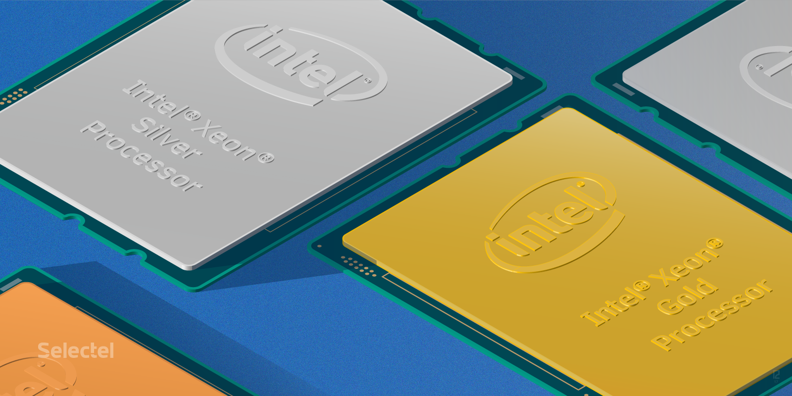
Dedicated Servers with Intel Xeon Skylake Scalable Processors
 On July 12, Intel presented its new line of server processors under the code name Skylake SP (Scalable Processors). This is no coincidence: Intel has introduced a lot of innovations and, as one review (Rus) noted, “tried to offer something for everyone.”
The SP processor line is part of the Purley server platform, which has been called the “biggest data center platform advancement in this decade”.
Servers built on these new processors are already available for preorder in our data centers.
What innovations do we see with the Intel Skylake SP? What specs do these processors have? What advantages do these processors have over previous models? We’ll take a detailed look at all of these questions below.
New Processors – New Names
Previous lines of Xeon processors were given names with the format Exvx: E3v3, E3v5, etc. The SP family uses a different naming scheme: all of the processors are divided into four series, each named after a precious metal: Bronze, Silver, Gold, and Platinum. These series are differentiated by the number of cores and technology available.
Bronze processors are the most basic: they can have up to 8 cores and don’t support hyper-threading. Platinum processors, as the name suggests, were designed for extreme workloads and have the most cores (up to 28).
The names of some models also have an index. F indicates an integrated Omni-Path controller, M — high memory support (up to 1.5 TB per socket), and T — NEBS (Network Equipment Building System) support. Processors with the T index can sustain high-temperatures and have a longer life cycle longer compared to other models.
We’ll take a closer look at these below.
Technical Specifications
We offer configurations with the Intel Xeon Silver 4114 and Intel Xeon Gold 6140 processors. Their basic specs are given in the table below:
| Characteristic | Intel Xeon Silver 4114 | Intel Xeon Gold 6140 |
|---|---|---|
| Lithography | 14 nm | 14 nm |
| No. of cores | 10 | 18 |
| No. of threads | 20 | 36 |
| Base frequency | 2.20 GHz | 2.30 GHz |
| Max Turbo Frequency | 3.00 GHz | 3.70 GHz |
| L3 cache size | 13.75 MB | 24.75 MB |
| No. of UPI links | 2 | 3 |
| TDP (thermal design power) | 85 W | 140 W |
Primary Innovations
The most significant innovations introduced in the Skylake SP are:
- the AVX-512 instruction set significantly improves performance for integer and floating-point operations
- 6-channel memory controller (previous processors offered a max of 4 channels)
- UPI (Ultra Path Interconnect) technology accelerates communication between processor cores
- increased number of PCI lanes (up to 48)
- modified topology: the ring bus has been replaced by a mesh architecture
Microarchitecture
The SP line of processors has the same basic core structure as the previous Skylake models. Nevertheless, there are a few differences and some improvements have been made. The L2 cache has been increased to 1 MB and the L3 cache is now 13.75 MB per CPU core. The L2 cache is filled directly from the RAM and then unused lanes force that data to the L3. Data shared between cores is stored in the L3 cache.
We should point out that the size of the L3 cache does not depend on the number of cores; 8-core, 12-core, and even 18-core models (see above) have a cache of 24.75 MB.
As has been noted in numerous reviews, major emphasis has been given to the L2 cache. The previously used built-in eDRAM is completely absent from the Skylake processors.
New Topology
An important innovation in the Intel Skylake SP processors is the lack of an on-chip ring bus, which was used for 10 years to facilitate communication between cores.
The first ring buses appeared in 2009 in the 8-core Nehalem-EX processors. They proved to be efficient (up to 3 GHz) and the L3 cache experienced minimal lag. If the core found data in its cache fragment, it required only one additional cycle. To retrieve the cache line from another fragment, it required up to 12 cycles (6 cycles on average).
Consequently, ring bus technology underwent a multitude of changes and improvements. The Ivy Bridge processors, which were released in 2012, had three rows of cores interconnected by a bi-directional two ring bus system (one moved clockwise, the other counterclockwise), which let them deliver their loads along a shorter route, lowering latency. When data entered the ring structure, their path needed to be coordinated to avoid mixing with previous data.
Things got even more complicated with the Intel Xeon E5v3 processors (2014): four rows of cores, two mutually independent ring buses, and a buffer switch.
Ring bus technology was fairly widespread when processors had a maximum of 8 cores. However, when processors with over 20 cores started to appear, it became clear that its possible application was coming to a close. Of course, the easiest solution would have been to add one more ring, bringing the total to three. But Intel decided to take a different approach and switch to a new ring structure — mesh. This approach had already been tried with the Xeon Phi processors (more information can be found here).
We can visualize the mesh topology of the bus structure as follows:
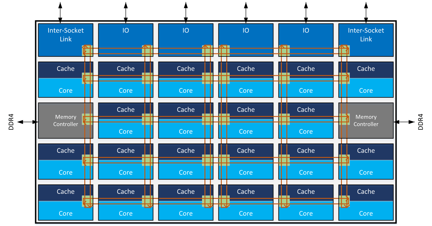
Illustration courtesy of Intel
Thanks to this new topology, cores interact with one another much faster than before and memory operations are more streamlined.
New AVX-512 Instruction Sets
Computing performance in Skylake SP processors has improved thanks to the use of the new AVX-512 instruction set. It expands 32-bit and 64-bit AVX instructions by using 512-bit vectors.
Programs can now pack eight floating point double precision integers or sixteen single precision floating point integers, as well as eight 64-bit or sixteen 32-bit integers within 512-bit vectors. This enables processing of twice the number of data elements that AVX/AVX2 can process with a single instruction and four times that of SSE.
The AVX-512 is fully compatible with the AVX instruction set. This means that both instruction sets can be used in one program without performance penalties (which was the case when using SSE and AVX together). The AVX registers (YMM0-YMM15) map into the AVX-512 registers (ZMM0-ZMM15), similar to how SSE registers map into AVX registers. This is why in AVX-512 supported processors, AVX and AVX2 instructions operate on the lower 128 or 256 bits of the first 16 ZMM registers.
Performance Benchmarks
Sysbench
No review of a new processor would be complete without performance benchmark results. We compared two servers: one built on the Intel Xeon 8170 Platinum and the other built on the Intel Xeon E5-2680v4. Ubuntu 16.04 was installed on both servers.
We’ll start with the popular sysbench tests.
The first benchmark we checked was a simple integer search.
We installed sysbench on both servers and ran the following command:
sysbench --test=cpu --cpu-max-prime=200000 --num-thread=1 run
During the course of the test, we increased the number of threads (num-threads parameter) from 1 to 100.
The results of the test are visualized in the graphic below (the lower the number, the better the result):
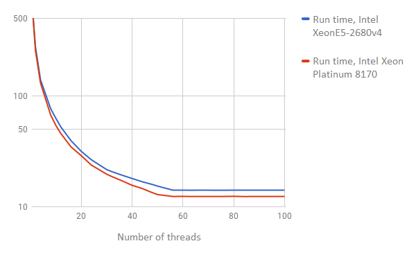
By increasing the number of threads, the Intel Platinum 8170 yielded better results.
Let’s now look at the results of an I/O buffer operations speed (the lower the number, the better the result):
Here we see a similar picture: by increasing the number of threads, the Intel Xeon 8170 Platinum comes out on top.
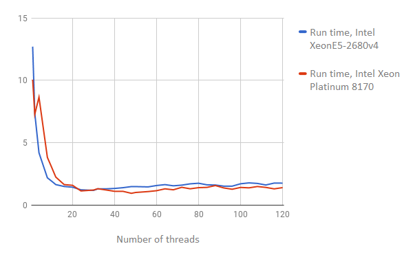
The threads test checks operations with a large number of competing threads. During our experiment, we increased the number of threads from 1 to 120.
These results are presented below (the lower the number, the better the result):
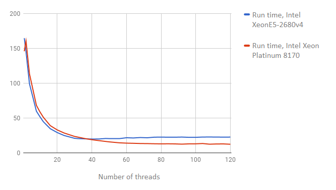
As we can see in the graph, increasing the number of threads yielded higher results for the Intel Skylake SP Platinum processor.
Linpack
The next benchmark we ran was Linpack. This test is used for measuring performance of computations with floating points and is the de-facto standard in the field of computational system testing. This is the benchmark used to create the list of the most powerful systems in the world.
For this benchmark, a system of linear equations is solved using LU decomposition. Performance is measured in flops, which is short for floating-point operations per second. You can find more information about the algorithm Linpack is based on here.
The Linpack benchmark can be downloaded on the Intel site. During the test, the program solves 15 equation systems with different size matrices (from 1000 to 45000). The results of our test are presented below (the higher the number, the better the result):
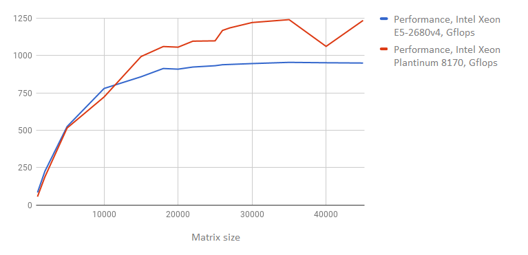
As we can see, the new processor yields much higher results. When testing the largest matrix size (45,000), performance for the Intel Xeon E5-2680v4 came to 948.9728 Gflops, and the Intel Xeon Platinum to 1233.2960 Gflops.
Boost Compile Speed Test
When assessing a processor’s performance, it’s preferable to run not only benchmarks, but to tests that best simulate real-world applications. This is why we decided to see how quickly our servers can compile a set of C++ Boost libraries from the source code.
We used the latest stable version of Boost — 1.64.0; the archive with the source code was downloaded from the official site.
The server with the Intel Xeon E5-2680v4 processor took 12 minutes 25 seconds to compile. The server built on the Xeon Platinum handled the task even faster in only 9 minutes 16 seconds.
Conclusion
In this article, we looked at the most significant innovations in the Intel Skylake Scalable processors. Servers with these new processors are already available for preorder in our data centers in St. Petersburg and Moscow.
We currently offer the following configurations:
| Processor | RAM | Storage |
|---|---|---|
| Intel Xeon Silver 4114 | 96 GB DDR4 | 2 × 480 GB SSD + 2 × 4 TB SATA |
| Intel Xeon Silver 4114 | 192 GB DDR4 | 2 × 480 GB SSD |
| Intel Xeon Silver 4114 | 384 GB DDR4 | 2 × 480 GB SSD |
| Intel Xeon Gold 6140 2.1 | 384 GB DDR4 | 2 × 800 GB SSD |
To lease these servers, you will have to fill out a preorder form, but they will soon be available on a permanent basis.